


News
Molecular pump factory Application of Molecular Pump in Semiconductor Equipment
- Categories:Molecular Pump factory
- Author:
- Origin:
- Time of issue:2022-05-07
- Views:0
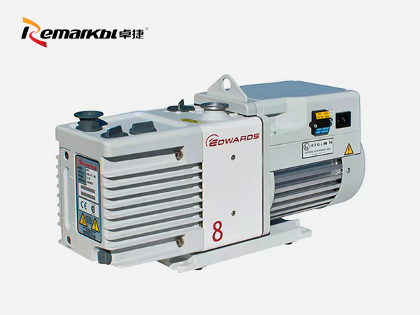
(Summary description)In the production process of molecular pump factory, molecular pump is widely used in key equipment such as lithography machine, thin film deposition equipment, etching equipment, ion implanter and so on.

Molecular pump factory Application of Molecular Pump in Semiconductor Equipment
(Summary description)In the production process of molecular pump factory, molecular pump is widely used in key equipment such as lithography machine, thin film deposition equipment, etching equipment, ion implanter and so on.
- Categories:Molecular Pump factory
- Author:
- Origin:
- Time of issue:2022-05-07
- Views:0
In the production process of molecular pump factory, molecular pump is widely used in key equipment such as lithography machine, thin film deposition equipment, etching equipment, ion implanter and so on.
Molecular pump factory talks about lithography machine
The lithography machine is the core equipment for the production of large-scale integrated circuits. Manufacturing and maintenance require a high level of optical and electronic industrial bases. Only a few molecular pump factories in the world master it, so the lithography machine is expensive.
The lithography process of the lithography machine in the molecular pump factory must be realized in a high vacuum environment, because the extreme ultraviolet light is very delicate and easily lost in the air. At the same time, during the lithography process, the action time error of the device is measured in picoseconds, which requires extremely high vibration value of the magnetic levitation molecular pump.
Molecular pump factory talks about thin film deposition equipment
Molecular Pump Factory believes that thin film deposition refers to the formation of various thin films on the surface of the wafer, which can be insulators, semiconductors or conductors. They are composed of different materials and are grown or deposited using a variety of processes. Common deposition techniques are chemical vapor deposition (CVD), evaporation and sputtering PVD.
Generally speaking, a heat treatment process such as a low temperature (≤500°C) annealing process is also included to improve the low resistance contact between the metal layer and the semiconductor and eliminate internal stress. Molecular pump plant equipment requires a high-clean vacuum environment during the operation process, generally using an oil-free vacuum system based on a magnetic levitation molecular pump.
Scan the QR code to read on your phone

Conatct
Tel:+86 18930867676
Add: Room 1820, Block B, Red Star World Trade Building, No.598, Nujiang North Road, Putuo District, Shanghai

Jobs
Zapa always believes that talents are the invincibility of the company in the market
Core resources
Talent Concept
Zapa always believes that talents are the invincibility of the company in the market
Core resources
Copyright:Shanghai ZaPa Vacuum Technology Co., Ltd. - 2020 All Rights Reserved. 沪ICP备18006805号 Designed By:www.300.cn
